Silicon Supply Chain: The Hidden Price of Bypassing EUV Restrictions
Chinese manufacturers are using older DUV tools to produce advanced chips, but experts warn that the lack of extreme ultraviolet light drives up costs and reduces efficiency significantly.
By Madison Darwish ·
For consumers and businesses relying on high-performance computing, the hardware underpinning modern technology is becoming more expensive to produce. This is not due to a shortage of silicon wafers, but rather a specific limitation in the manufacturing equipment available to Chinese foundries. While export controls have prevented the country from accessing the most advanced lithography tools, manufacturers have found a way to build capable processors using older machinery. The tradeoff, however, is a significant increase in production complexity and cost for every chip that leaves the factory.
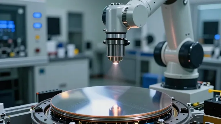
The core of the issue lies in the availability of extreme ultraviolet lithography machines, which are produced exclusively by ASML. These tools use light with a wavelength of 13.5 nanometers to print extremely fine details onto chips. Without them, Chinese firms must rely on deep ultraviolet equipment. Analysts suggest this technological gap places China roughly five years behind Western competitors in terms of cutting-edge manufacturing capability. This deficit creates a persistent bottleneck for those seeking to produce the most advanced logic chips available on the global market.
Despite these constraints, recent evidence shows that Chinese manufacturers have made substantial strides. A teardown of the Huawei Mate 60 Pro revealed that its processor was built by SMIC using a seven-nanometer class process that did not require EUV. Further analysis of the newer Kirin 9030 chip indicates that SMIC has pushed its DUV-based methods to densities approaching five-nanometer levels. While this still trails the leading processes from TSMC and Samsung, it demonstrates a clear ability to advance without the newest tools. The method relies on multiple patterning, where a single complex layer is broken into several simpler steps and built up sequentially.
This step-by-step approach introduces significant financial and technical penalties. Chris Mack, a semiconductor expert, notes that industry standards suggest three exposures on older immersion tools cost about the same as one EUV pass. However, once the process requires four or more masks, the older method becomes more expensive. Quality control also suffers because each new pattern must align perfectly with the previous ones. Misalignment leads to defects, forcing designers to add extra space around components. This enlarges the chip and reduces the number of usable dies per wafer, which is a costly outcome given that each wafer can cost tens of thousands of dollars. As Mack pointed out, manufacturers do not sell wafers; they sell individual dies.
The efficiency gap is particularly visible in memory production. A June report from Morgan Stanley estimated that Chinese DRAM maker CXMT produces only one-third as many bits per wafer as its Western rivals. The bank described access to lithography as a hard ceiling for Chinese memory development. Experts also caution that node labels like 5nm or 3nm are not definitive measures of capability. SMIC’s N+3 process represents progress, but it remains significantly less scaled than the established five-nanometer processes from major Western and Asian competitors.
There is still room to optimize the DUV approach. Micron previously developed its 1-alpha DRAM without EUV by using tight process control and multiple patterning. Mack noted that Micron pushed the older technology further than most other memory makers. Morgan Stanley believes CXMT can achieve a similar level for its planned HBM3e products. Researchers from Copenhagen Business School expect that advanced packaging techniques will allow firms to use DUV for the latest DRAM generations by the end of the decade. If China secures the full ecosystem for 193 immersion tools and designs products around them, they can make significant headway, though memory is generally easier to scale than logic chips.
The outlook suggests that Chinese chipmakers will not stop growing, but they will face persistent economic headwinds. They may continue to expand capacity while accepting larger dies, lower yields, or longer manufacturing times. Morgan Stanley projects that CXMT will increase its share of global DRAM bit supply from 14% in 2026 to 16% by 2028, primarily through new production sites. The bank also expects China’s self-sufficiency in AI chips to rise from 42% in 2025 to 70% by 2030. However, a gap will likely remain in areas requiring EUV, high-bandwidth memory, and advanced software.
Source: Tom's Hardware